A milliohmmeter is just the tool for checking trace resistance on a printed circuit board, tracking down shorted traces, and measuring the contact resistance of a switch or connector. Its the kind of tool that would come in real handy occasionally, but not often enough to justify shelling out hundreds of dollars. Wanting one anyway, I set out to make my own. It turned out to be not only an exciting project, but a true adventure of discovery as it provided a window into the workings of lock-in amplifiers. With a lock-in amplifier topology, a microcontroller and a little firmware makes the venerable (if somewhat noisy) LM324 bipolar op-amp provide high gain and at the same time reduces noise. Improve analog performance with a microcontroller? Now THIS is a fun project!
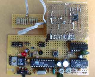
My main concern in the milliohmmeter design was how to get stable resistance readings with a suitably low test current. After all, I wanted to look at a few or few tens of milliohms, but I wanted to keep the test current low so as not to exceed the current ratings of some of the parts I want to test, and so I can run it all from a battery. For starters, 25 milliamps x 1 milliohm = 25 microvolts. This meant that I would have to be able to measure and display voltages in the range of tens of microvolts per count in a stable and repeatable manor. I also wanted the circuit to be forgiving of my hand wired breadboards, shown in photo 1. That is what lead me to the lock-in amplifier.
The Wonder Of Lock-In Amplification

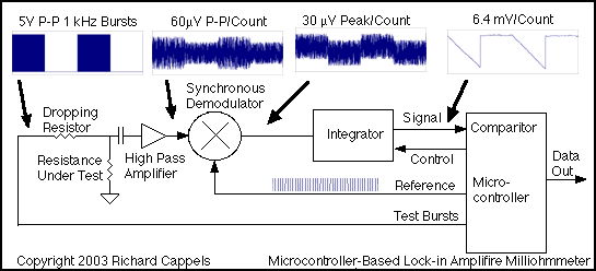
Figure 1 The lock-in amplifier detects and integrates bursts of 1 kHz pulses that result from the IR drop across the resistance under test. The result is 46 db of signal gain while vastly improving the signal-to-noise ratio. The preamplifier doubles as a high-pass filter to remove the DC component of the pulses and reduce flicker burst noise from the op-amp.
A lock-in amplifier provides gain for the signal at a specific frequency and phase, while reducing noise. Its almost like getting something for nothing, but that’s not really the case. Since you have to effectively average many measurements to improve the signal to noise ratio, what you are really doing is trading way bandwidth and responsiveness to improve the signal to noise ratio.
In this circuit, shown in the block diagram in figure 1, a 1 kHz burst of 5 volt peak pulses is applied to a series dropping resistor to establish a pulsing current through the resistance under test. The IR drop across the resistor under test is a voltage proportional to the value of the resistance. After passing through a high pass filter to eliminate the DC component of the signal, it is rectified by a synchronous demodulator. For a period of time corresponding to the burst, the rectified signal is applied to an integrator, which charges up, and then at the end of the burst, the time it takes the integrator to discharge at a constant rate is measured to determine the size of the charge, and that is how the average amplitude of the signal applied to the integrator is determined.
Since random noise is not synchronized with the switching in the synchronous demodulator, it is not rectified and it averages out to nearly zero. The longer the integration time, the less proportionate effect a given small pulse of noise has on the integrator’s output, and the more gain the integrator has for the 1 kHz burst. Integration is the wonder of lock-in .amplification.
While testing the circuit I was surprised that when leaving the input open circuited, the meter gave a very low resistance measurement. I spent a long time looking over the firmware, looking for math errors or register use conflicts, before I decided to take a look at the circuit with an oscilloscope. That’s when I saw that when the meter’s input terminals were unloaded, there was virtually no signal across the input terminals. Without the test resistance in series with the 220 Ohm resistor, there was no signal – the input just charged up to +5 volts and wiggled a little because of capacitive coupling between the transistor’s base and collector. That’s when I added the 10k resistor from the PNP’s collector to ground. I should have taken my early mentor’s advice, “Always look for the simplest explanation first.”
To make sure that I am only measuring the resistance of the thing I am trying to measure and not the resistance of my test leads, I used a 4 wire measurement system. In this system, two wires are used to deliver the test current and two separate wires are used to measure the voltage drop. Simple enough, but how did I keep the test current ground return path separate from the voltage sense ground line? There in lies much of the art in circuit layout. Looking at figure 2, the terminal marked “Test Current Return” connects directly to the battery’s negative connection to the circuit. The signal marked “Small Signal Return” connects to the rest of the analog circuits’ grounds, and then joins up with the battery ground at the point in the circuit where the 1.8 volt reference voltage is generated. The overall grounding scheme can be seen in figure 3.

